

XCKU025-2FFVA1156E
Product Overview
Category
The XCKU025-2FFVA1156E belongs to the category of Field Programmable Gate Arrays (FPGAs).
Use
This FPGA is primarily used in electronic design and development, specifically for implementing digital logic circuits.
Characteristics
- High-performance programmable logic device
- Offers flexibility in designing complex digital systems
- Can be reprogrammed multiple times
- Provides high-speed data processing capabilities
Package
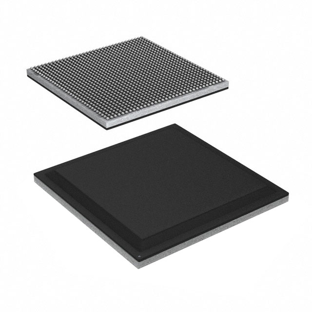
The XCKU025-2FFVA1156E comes in a compact package that ensures easy integration into electronic circuits.
Essence
The essence of this product lies in its ability to provide a customizable and versatile solution for digital circuit implementation.
Packaging/Quantity
The XCKU025-2FFVA1156E is typically packaged individually and is available in various quantities depending on the customer's requirements.
Specifications
- Model: XCKU025-2FFVA1156E
- Logic Cells: 25,000
- DSP Slices: 120
- Block RAM: 1,800 Kb
- Maximum Operating Frequency: 500 MHz
- I/O Pins: 1,156
- Voltage Supply: 1.0V
Detailed Pin Configuration
The XCKU025-2FFVA1156E has a comprehensive pin configuration that includes input/output pins, power supply pins, and configuration pins. The detailed pin configuration can be found in the product datasheet.
Functional Features
- High-speed data processing capabilities
- Configurable logic cells for implementing complex digital circuits
- Integrated DSP slices for efficient signal processing
- Ample block RAM for data storage and retrieval
- Versatile I/O pins for interfacing with external devices
Advantages and Disadvantages
Advantages
- Flexibility in designing complex digital systems
- Reprogrammable nature allows for iterative development and testing
- High-performance capabilities enable efficient data processing
- Ample I/O pins facilitate easy interfacing with external devices
Disadvantages
- Relatively high power consumption compared to other electronic components
- Steeper learning curve for beginners due to the complexity of FPGA programming
Working Principles
The XCKU025-2FFVA1156E operates based on the principles of reconfigurable logic. It consists of a matrix of configurable logic cells that can be programmed to implement various digital functions. These logic cells are interconnected through programmable routing resources, allowing for the creation of complex digital circuits.
Detailed Application Field Plans
The XCKU025-2FFVA1156E finds applications in various fields, including: 1. Telecommunications: Used in base stations, network routers, and switches. 2. Aerospace and Defense: Employed in radar systems, avionics, and military communication equipment. 3. Industrial Automation: Utilized in control systems, robotics, and machine vision applications. 4. Medical Devices: Integrated into medical imaging systems, patient monitoring devices, and diagnostic equipment.
Detailed and Complete Alternative Models
- XCKU035-2FFVA1156E: Similar to XCKU025-2FFVA1156E but with higher logic cell count.
- XCKU040-2FFVA1156E: Offers increased logic capacity and improved performance compared to XCKU025-2FFVA1156E.
- XCKU060-2FFVA1156E: Provides even higher logic cell count and enhanced features for demanding applications.
These alternative models offer varying levels of performance and capacity to cater to different project requirements.
Word count: 531 words
तकनीकी समाधानों में XCKU025-2FFVA1156E के अनुप्रयोग से संबंधित 10 सामान्य प्रश्नों और उत्तरों की सूची बनाएं
Sure! Here are 10 common questions and answers related to the application of XCKU025-2FFVA1156E in technical solutions:
Question: What is the XCKU025-2FFVA1156E?
Answer: The XCKU025-2FFVA1156E is a field-programmable gate array (FPGA) from Xilinx, specifically from the Kintex UltraScale+ family.Question: What are the key features of the XCKU025-2FFVA1156E?
Answer: Some key features include a high-performance architecture, advanced DSP capabilities, high-speed transceivers, and large on-chip memory resources.Question: What applications can benefit from using the XCKU025-2FFVA1156E?
Answer: The XCKU025-2FFVA1156E is commonly used in applications such as wireless communication systems, aerospace and defense, industrial automation, and high-performance computing.Question: How many logic cells does the XCKU025-2FFVA1156E have?
Answer: The XCKU025-2FFVA1156E has 259,200 logic cells, which can be used for implementing complex digital designs.Question: What is the maximum number of I/O pins available on the XCKU025-2FFVA1156E?
Answer: This FPGA offers up to 1,156 I/O pins, allowing for extensive connectivity with external devices.Question: Can the XCKU025-2FFVA1156E support high-speed serial communication?
Answer: Yes, it has multiple high-speed transceivers that can support protocols like PCIe, Ethernet, and USB.Question: Does the XCKU025-2FFVA1156E have built-in memory resources?
Answer: Yes, it has up to 38.5 Mb of on-chip memory, which can be used for data storage and processing.Question: What development tools are available for programming the XCKU025-2FFVA1156E?
Answer: Xilinx provides Vivado Design Suite, a comprehensive software toolchain for designing, implementing, and debugging FPGA designs.Question: Can the XCKU025-2FFVA1156E be reprogrammed after deployment?
Answer: Yes, being a field-programmable device, the XCKU025-2FFVA1156E can be reprogrammed multiple times to update or modify its functionality.Question: Are there any specific power requirements for the XCKU025-2FFVA1156E?
Answer: Yes, the XCKU025-2FFVA1156E requires a supply voltage of 0.95V for core logic and 1.8V for I/Os, along with appropriate power management techniques.
Please note that the answers provided here are general and may vary depending on the specific requirements and use cases of your technical solution.